The electric vehicle conversation tends to focus on batteries. Range, charging speed, cost per kilowatt-hour, chemistry. These are the metrics that dominate headlines and shape consumer decisions. But behind every one of those metrics sits a less visible technology that determines how efficiently the battery’s energy is used, how fast it can be replenished, and how much space the power electronics consume inside the vehicle.
That technology is the wide band gap semiconductor. Silicon carbide and gallium nitride are not new materials. They have been studied for decades. But their adoption in electric vehicles is accelerating rapidly in 2026, driven by the shift to 800-volt architectures, the demand for faster charging, and the relentless pressure to reduce cost and weight.
This is the hidden technology accelerating EV adoption: wide band gap semiconductors, and why they matter more than most drivers realize.
What Wide Band Gap Actually Means
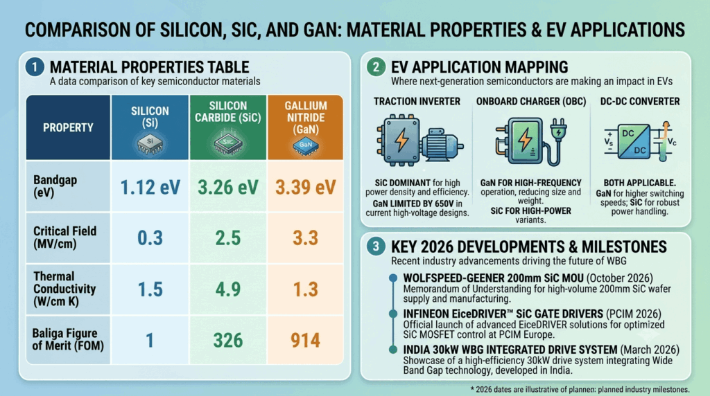
The term “band gap” refers to the energy required to move an electron from the valence band to the conduction band in a semiconductor material. Silicon, the workhorse of the semiconductor industry, has a band gap of 1.12 electron volts. Silicon carbide (4H-SiC) has a band gap of 3.26 eV. Gallium nitride has a band gap of 3.39 eV . That difference, roughly three times wider, is the source of every advantage WBG materials offer.
The wider band gap translates into a higher critical electric field. Silicon’s critical field is 0.3 MV/cm. SiC reaches 2.5 MV/cm. GaN reaches 3.3 MV/cm . This means a WBG device can block the same voltage with a much thinner and more lightly doped drift region. The result is dramatically lower on-resistance per unit area.
The Baliga figure of merit, which quantifies a material’s suitability for power devices, places SiC at 326 times silicon and GaN at 914 times silicon . These are not incremental improvements. They represent a fundamental shift in what is physically possible in power conversion.
At a 1200-volt rating, the silicon limit for specific on-resistance is approximately 147 milliohm-square-centimeters. SiC achieves 0.45, and GaN achieves 0.16 . Real devices sit above these theoretical limits due to channel, substrate, and contact resistances. But the direction and magnitude of the advantage are clear.
The 800-Volt Transition and Why It Needs WBG
The automotive industry is shifting from 400-volt to 800-volt architectures. Porsche pioneered the transition with the Taycan, and Hyundai, Kia, Audi, Lucid, and others have followed. The 800-volt architecture enables faster charging because power is the product of voltage and current. Doubling the voltage halves the current required for the same charging power, reducing resistive losses and allowing thinner cables.
But 800 volts also places greater demands on the power semiconductors. Silicon IGBTs, which dominated 400-volt systems, become less efficient at higher voltages. Their switching losses increase, and their thermal performance becomes a constraint. This is where WBG materials become essential rather than optional.
A review paper published in June 2026 described the transition directly: the automotive industry is undergoing a pivotal transformation as electric vehicles shift from traditional 400V silicon-based systems toward high-efficiency 800V architectures. While silicon IGBTs have long been the industry standard, they face physical limits regarding switching speeds and heat. WBG materials like SiC and GaN enable faster charging, increased driving range, and more compact designs .
The efficiency gains are substantial. An IEEE technical talk in July 2026 noted that WBG devices enable 98% inverter efficiency and sub-20-minute charging in 800V architectures . For a vehicle consuming 15 kWh per 100 kilometers, a 2% improvement in inverter efficiency translates to roughly 0.3 kWh saved per 100 kilometers. Over 200,000 kilometers, that is 600 kWh of energy that does not need to be stored in the battery, charged, or paid for.
Silicon Carbide: The Incumbent WBG Material for Traction
Silicon carbide is currently the dominant WBG material in EV traction inverters. Its thermal conductivity, 4.9 W/cm K compared with silicon’s 1.5, allows it to dissipate heat more effectively, reducing the cooling burden and enabling more compact designs . Its critical field and on-resistance advantages allow inverters to operate at higher voltages and frequencies with lower losses.
The commercial ecosystem around SiC is maturing rapidly. In October 2026, Wolfspeed signed a memorandum of understanding with Chinese power module manufacturer Geener Microelectronics. Under the agreement, Geener’s next-generation power module platform will prioritize Wolfspeed’s SiC bare die for applications including new energy vehicle main inverters. The two companies will jointly approach Chinese automakers with high-voltage electric platforms, aiming to secure design wins .
The significance of the deal lies partly in Wolfspeed’s 200mm SiC production line. Compared with 6-inch wafers, 8-inch (200mm) wafers can reduce per-chip costs by approximately 30% . That cost reduction is the key to moving SiC from premium vehicles into mainstream models, and from automotive applications into broader industrial and data center markets.
At PCIM Europe 2026, Infineon launched its EiceDRIVER gate drivers for battery-electric vehicle traction inverters. The 1EDI3040AS and 1EDI3041AS support both IGBTs and SiC MOSFETs, featuring real-time gate current adjustment to balance switching speeds against electromagnetic interference and precise control over switching transitions to reduce turn-on and turn-off energy dissipation . The gate driver is a critical but often overlooked component. A SiC MOSFET without an appropriate gate driver cannot deliver its theoretical advantages in a real inverter.
Gallium Nitride: The Challenger With a Different Niche
Gallium nitride offers even higher theoretical performance than SiC. Its Baliga figure of merit is nearly three times higher, and its critical field is higher. But its material properties and device architecture lead it to different applications.
Commercial GaN power transistors are mostly lateral high-electron-mobility transistors grown on silicon or other foreign substrates. The lateral structure limits voltage scaling, and commercial GaN parts are mostly at or below 650 volts . That voltage range is well-suited to 400-volt systems and onboard chargers, but less suited to 800-volt traction inverters, where SiC’s vertical structure and higher voltage capability have an advantage.
GaN’s strength is high-frequency switching. Because GaN devices do not have an intrinsic body diode like silicon and SiC MOSFETs, they can operate at much higher frequencies at room temperature. This allows the use of smaller passive components, reducing the size and weight of onboard chargers and DC-DC converters . A 6.6 kW bidirectional onboard charger using GaN technology has been projected to achieve above 96% peak efficiency .
Infineon’s GaN strategy illustrates the state of the market. The company acquired GaN Systems in 2023, but is now phasing out those automotive parts because GaN Systems built its devices at TSMC, which is shutting down its GaN foundry business. Infineon is developing its own 650V automotive GaN parts and expects the first GaN in onboard chargers later this year, with revenue starting in the next 12 to 18 months . The transition is not a setback for GaN in automotive. It is a sign that the technology is moving from acquisition-driven portfolios to in-house manufacturing designed specifically for automotive qualification.
India’s Indigenous WBG Push
The WBG transition is not confined to established semiconductor powers. In March 2026, India’s Ministry of Electronics and IT launched a 30 kW wide band gap-based Integrated Drive System for electric vehicle applications, developed by C-DAC Thiruvananthapuram in collaboration with IIT Madras and Lucas TVS under the National Mission on Power Electronics Technology .
The 30 kW power class is particularly relevant to India’s electric passenger vehicle segment, including compact cars and fleet mobility platforms. A substantial portion of high-performance EV powertrain systems and semiconductor-based drive components are currently imported. Indigenous development of integrated drive systems is expected to reduce import dependence, lower system costs through localization, and support scalable manufacturing aligned with the Production-Linked Incentive schemes .
The Integrated Drive System combines the electric motor and inverter into a single compact, high-power-density unit, replacing the conventional separated motor-drive configuration . This is a system-level innovation that goes beyond the semiconductor itself. It demonstrates that WBG adoption is not only about replacing silicon with SiC or GaN. It is about rethinking the architecture of the entire powertrain around the capabilities that WBG devices enable.
What WBG Semiconductors Actually Deliver
The benefits of WBG semiconductors in electric vehicles can be summarized in four categories.
Efficiency. Lower conduction and switching losses mean more of the battery’s energy reaches the wheels. At the system level, this translates directly into range. A more efficient inverter can add tens of kilometers of range without any change to the battery pack.
Power density. WBG devices can handle higher voltages and currents in smaller packages. This reduces the size and weight of the inverter, onboard charger, and DC-DC converter, freeing up space for passengers or cargo and reducing the vehicle’s overall mass.
Thermal performance. SiC’s thermal conductivity is roughly three times that of silicon. This reduces the junction temperature for a given loss and eases the cooling design, which in turn reduces the size and cost of the thermal management system .
Charging speed. The combination of higher voltage capability and lower losses enables the high-power charging that 800-volt architectures promise. Without WBG devices, the charging speeds that consumers now expect from premium EVs would not be achievable in a practical package.
The Challenges That Remain
The WBG transition is not without obstacles. Cost is the most significant. SiC substrates are more expensive to produce than silicon wafers, and the manufacturing processes are less mature. The shift to 200mm wafers is reducing costs, but the gap with silicon remains.
Gate driving complexity is another challenge. WBG devices switch faster, which means they are more sensitive to parasitic inductance and require more precise gate control. Infineon’s EiceDRIVER launch at PCIM 2026 was a direct response to this challenge, integrating features that would otherwise require external circuitry .
Reliability and functional safety are ongoing concerns. Automotive qualification requires demonstrating performance over the full lifetime of the vehicle, across temperature extremes, and under fault conditions. The ISO 26262 functional safety standard imposes requirements on torque control, thermal protection, and electrical insulation that WBG systems must meet .
The supply chain is also evolving. The Wolfspeed-Geener agreement, the Infineon GaN transition, and the India indigenous drive system all reflect a market that is still forming its industrial structure. The companies that secure design wins and manufacturing scale in the next few years will define the competitive landscape for the next decade.
What This Means for EV Buyers
For consumers, WBG semiconductors are invisible. They do not appear on specification sheets. They are not mentioned in advertising. But their impact is felt in every metric that buyers care about.
A vehicle with a SiC inverter charges faster, drives further on the same battery, and weighs less than an equivalent vehicle with a silicon inverter. The difference may be a few percent in each category, but those few percent compound. They determine whether a vehicle meets a range target, whether it can charge in under 20 minutes, and whether it can be priced competitively.
The WBG transition is also a story about the maturation of the EV industry. The first generation of electric vehicles competed on the novelty of electrification. The second generation competed on battery cost and range. The third generation is competing on efficiency, and efficiency is where WBG semiconductors matter most.
The hidden technology accelerating EV adoption is not hidden because it is secret. It is hidden because it operates behind the scenes, inside the inverter and the onboard charger, converting and controlling the energy that the battery stores. But its impact is visible in every vehicle that charges quickly, drives efficiently, and competes on price with a petrol equivalent.
The WBG era in electric vehicles has arrived. It is just not the part of the story that gets the headlines.